What is Pure Indium Used for?
Table of Contents
Introduction
Mostly utilized in the production of indium tin oxide (ITO) for touch screens, flat-panel displays, and solar panels, indium also contributes to advancements in semiconductors and specialized alloys. This article explores the extraction, properties, and diverse applications of indium, emphasizing its impact on technological innovation.
Properties and Extraction of Indium
Indium is a soft, silvery metal characterized by its remarkable stability and adaptability. Its extraction typically involves refining indium-bearing zinc or tin ores, using advanced statistical process control techniques to achieve high purity levels. This ensures its suitability for both industrial and technological applications.
Key Physical Properties of Indium
| Property | Description |
|---|---|
| Stability | Resistant to oxidation in air and water |
| Conductivity | Excellent electrical and thermal conductance |
| Adhesion | Bonds strongly to glass |
| Malleability and Ductility | Maintains flexibility at low temperatures |
Applications in Modern Technology
Indium Tin Oxide (ITO): A Transparent Conductor
Indium’s most widespread application is in the production of indium tin oxide (ITO), a material vital for:
Touch Screens and Displays: ITO’s transparency and conductivity make it essential for touch-sensitive devices and flat-panel displays.
Solar Panels: Acts as a conductive layer, enhancing photon conversion efficiency.
ITO’s combination of transparency, conductivity, and durability underpins its dominance in display technologies and renewable energy solutions.
Advanced Alloys and Low-Temperature Applications
Cryogenic Sealing: Remains malleable and ductile at temperatures below −150°C, ensuring reliable performance in extreme conditions.
Soldering and Fusing: Alloys with melting points between 6.5°C and 310°C are used in precision soldering applications.
Cooling Solutions for High-End Devices
Indium is also employed in thermal management solutions. By reducing operating temperatures by up to 10°C, it enhances the performance and longevity of high-end electronics.
Role in Semiconductor Technology
Indium shows semiconducting properties, making it indispensable in the development of advanced electronic and optoelectronic devices. Key applications include:
Solar Energy: Used as an absorber layer in solar panels, converting sunlight into electricity.
Compound Semiconductors: Integral to materials like InAs, InGaAs, and InGaN for integrated circuits, lasers, and LEDs.
Next-Generation Displays: IGZO (indium, gallium, and zinc oxides) is increasingly used for pixel switching transistors in cutting-edge displays.
Evaporative Deposition Techniques
Indium pellets and shot are utilized in evaporative methods to form active layers in various electronic components, further expanding its application potential.
Conclusion
Indium’s combination of metallic and semiconducting properties positions it as a cornerstone material in modern technology. From enabling touch-sensitive interfaces and high-efficiency solar panels to advancing semiconductor applications, indium continues to drive innovation across industries. For more details, please contact our Sales or Technical Team.
Leave a Comment
Top Categories
Hot Product
Related Blog
Welcome to our blog dedicated to the attractive world of rare metal materials.

Order Status Before the Chinese New Year Holiday 2025
As the traditional Chinese New Year is approaching, please be informed that our company will start the holiday from January 25th.

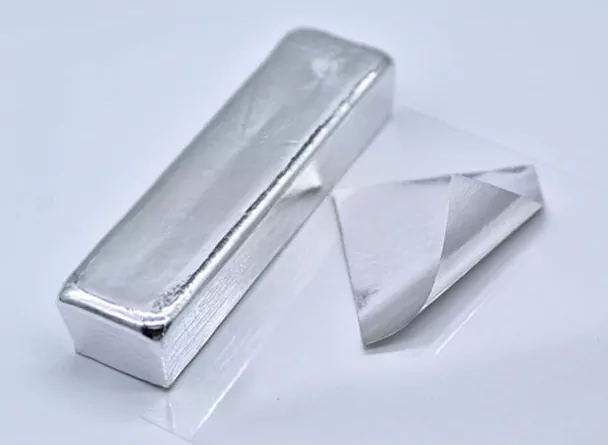
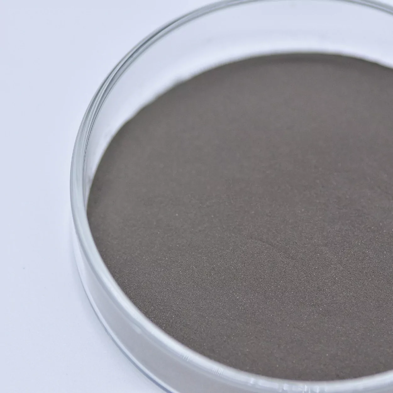
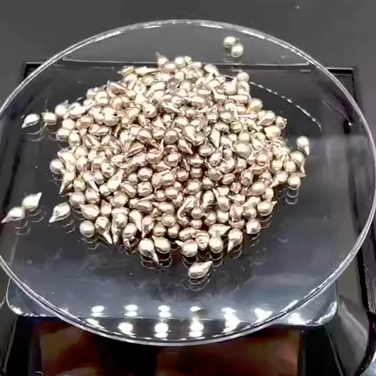
How to Extract and Use High Purity Tellurium
High purity tellurium is one of seven rare scattered metals, which are generally associated minerals and independent deposits are rare, as is tellurium.

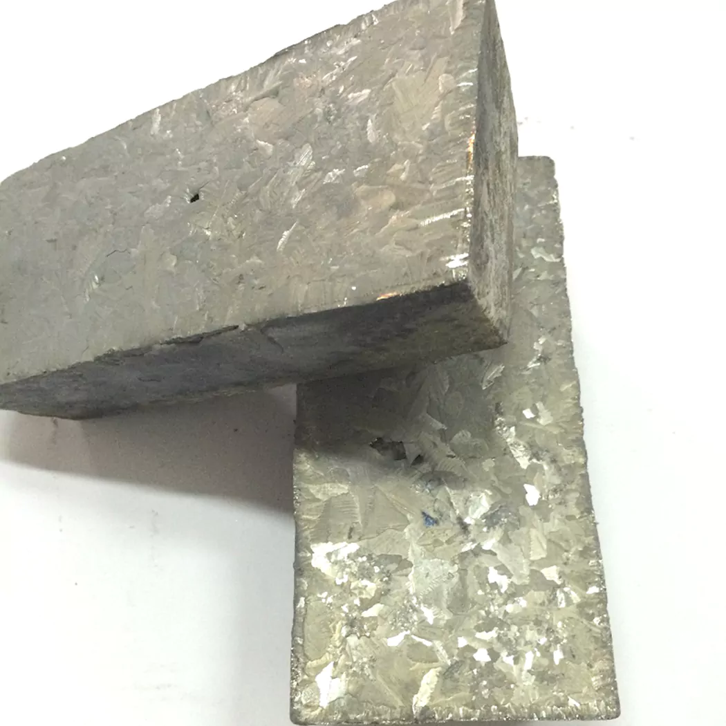
Why Has Bismuth Shot Cost Been Skyrocketing Recently
The market cost of bismuth shot has increased significantly in the past week as raw material 99.99% refined bismuth ingot was increased by USD600 per ton compared with last Wednesday.


